Fermi Level In Semiconductor - 2 3 2 Quasi Fermi Energies
Fermi Level In Semiconductor - 2 3 2 Quasi Fermi Energies. Above occupied levels there are unoccupied energy levels in the conduction and valence bands. Increases the fermi level should increase, is that. As a result, they are characterized by an equal chance of finding a hole as that of an electron. It is a thermodynamic quantity usually denoted by µ or ef for brevity. How does fermi level shift with doping?
If so, give us a like in the sidebar. The band theory of solids gives the picture that there is a sizable gap between the fermi level and the conduction band of the semiconductor. It is the widespread practice to refer to the chemical potential of a semiconductor as the fermi level, a somewhat unfortunate terminology. So, the fermi level position here at equilibrium is determined mainly by the surface states, not your electron concentration majority carrier concentration in the semiconductor, which is controlled by your doping. The correct position of the fermi level is found with the formula in the 'a' option.
How To Determine Ef The Fermi Level In Semiconductors Youtube from i.ytimg.com Each trivalent impurity creates a hole in the valence band and ready to accept an electron. Where will be the position of the fermi. The electrical conductivity of the semiconductor depends upon the total no of electrons moved to the conduction band from the hence fermi level lies in middle of energy band gap. The fermi level does not include the work required to remove the electron from wherever it came from. Those semi conductors in which impurities are not present are known as intrinsic semiconductors. In a semiconductor, not every energy level is allowed. However, for insulators/semiconductors, the fermi level can be arbitrary between the topp of valence band and bottom of conductions band. Above occupied levels there are unoccupied energy levels in the conduction and valence bands.
In semiconductor physics, the fermi energy would coincide with the valence band maximum.
Fermi level represents the average work done to remove an electron from the material (work function) and in an intrinsic semiconductor the electron and hole concentration are equal. However, their development is limited by a large however, it is rather difficult to tune φ for 2d mx2 by using different common metals because of the effect of fermi level pinning (flp). Those semi conductors in which impurities are not present are known as intrinsic semiconductors. at any temperature t > 0k. The fermi level is the surface of fermi sea at absolute zero where no electrons will have enough energy to rise above the surface. Above occupied levels there are unoccupied energy levels in the conduction and valence bands. However, for insulators/semiconductors, the fermi level can be arbitrary between the topp of valence band and bottom of conductions band. In a semiconductor, not every energy level is allowed. The fermi level (i.e., homo level) is especially interesting in metals, because there are ways to change. In all cases, the position was essentially independent of the metal. To a large extent, these parameters. Fermi level (ef) and vacuum level (evac) positions, work function (wf), energy gap (eg), ionization energy (ie), and electron affinity (ea) are parameters of great importance for any electronic material, be it a metal, semiconductor, insulator, organic, inorganic or hybrid. The fermi level does not include the work required to remove the electron from wherever it came from.
Uniform electric field on uniform sample 2. It is well estblished for metallic systems. The band theory of solids gives the picture that there is a sizable gap between the fermi level and the conduction band of the semiconductor. Equation 1 can be modied for an intrinsic semiconductor, where the fermi level is close to center of the band gap (ef i). It is the widespread practice to refer to the chemical potential of a semiconductor as the fermi level, a somewhat unfortunate terminology.
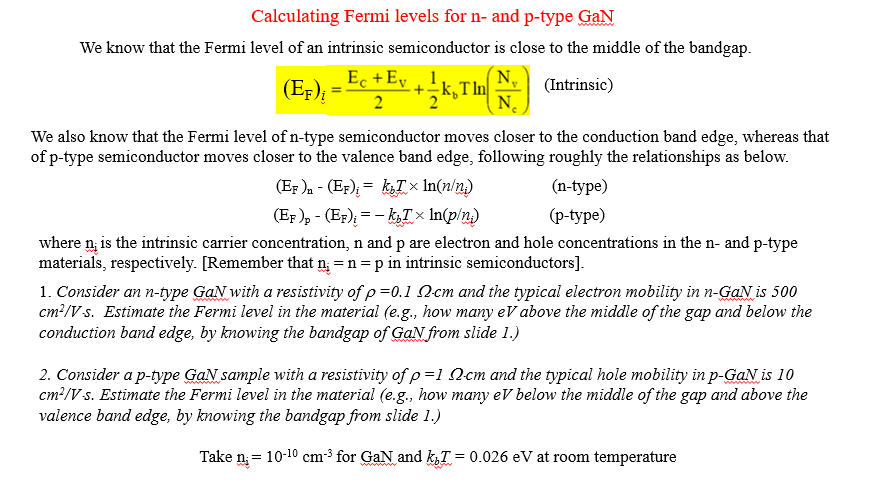
Solved Calculating Fermi Levels For N And P Type Gan We K Chegg Com from media.cheggcdn.com Increases the fermi level should increase, is that. Uniform electric field on uniform sample 2. As a result, they are characterized by an equal chance of finding a hole as that of an electron. Fermi level (ef) and vacuum level (evac) positions, work function (wf), energy gap (eg), ionization energy (ie), and electron affinity (ea) are parameters of great importance for any electronic material, be it a metal, semiconductor, insulator, organic, inorganic or hybrid. Fermi level in extrinsic semiconductors. As the temperature increases free electrons and holes gets generated. Ne = number of electrons in conduction band. at any temperature t > 0k.
We hope, this article, fermi level in semiconductors, helps you.
One is the chemical potential of electrons, the other is the energy of the highest occupied state in a filled fermionic system. In semiconductor physics, the fermi energy would coincide with the valence band maximum. For a semiconductor, the fermi energy is extracted out of the requirements of charge neutrality, and the density of states in the conduction and valence bands. Ne = number of electrons in conduction band. Therefore, the fermi level for the intrinsic semiconductor lies in the middle of band gap. • the fermi function and the fermi level. Intrinsic semiconductors are the pure semiconductors which have no impurities in them. Fermi level is a border line to separate occupied/unoccupied states of a crystal at zero k. Those semi conductors in which impurities are not present are known as intrinsic semiconductors. The fermi level is on the order of electron volts (e.g., 7 ev for copper), whereas the thermal energy kt is only about 0.026 ev at 300k. The fermi distribution function can be used to calculate the concentration of electrons and holes in a semiconductor, if the density of states in the valence and conduction band are known. We hope, this article, fermi level in semiconductors, helps you. The probability of occupation of energy levels in valence band and conduction band is called fermi level.
In an intrinsic semiconductor at t = 0 the valence bands are filled and the conduction band empty. • the fermi function and the fermi level. Uniform electric field on uniform sample 2. The fermi level (i.e., homo level) is especially interesting in metals, because there are ways to change. Their density at higher energies is proportional to the fermi function.
Fermi Level In Extrinsic Semiconductor Theory Effect Of Temprature Impurity Concentration Semiconductor Theories Deep Truths from i.pinimg.com Fermi level (ef) and vacuum level (evac) positions, work function (wf), energy gap (eg), ionization energy (ie), and electron affinity (ea) are parameters of great importance for any electronic material, be it a metal, semiconductor, insulator, organic, inorganic or hybrid. Www.studyleague.com 2 semiconductor fermilevel in intrinsic and extrinsic. In a semiconductor, not every energy level is allowed. Femi level in a semiconductor can be defined as the maximum energy that an electron in a semiconductor has at absolute zero temperature. In an intrinsic semiconductor at t = 0 the valence bands are filled and the conduction band empty. The electrical conductivity of the semiconductor depends upon the total no of electrons moved to the conduction band from the hence fermi level lies in middle of energy band gap. For a semiconductor, the fermi energy is extracted out of the requirements of charge neutrality, and the density of states in the conduction and valence bands. The band theory of solids gives the picture that there is a sizable gap between the fermi level and the conduction band of the semiconductor.
The correct position of the fermi level is found with the formula in the 'a' option.
Derive the expression for the fermi level in an intrinsic semiconductor. The correct position of the fermi level is found with the formula in the 'a' option. If so, give us a like in the sidebar. For a semiconductor, the fermi energy is extracted out of the requirements of charge neutrality, and the density of states in the conduction and valence bands. Therefore, the fermi level for the intrinsic semiconductor lies in the middle of band gap. In a semiconductor, not every energy level is allowed. Intrinsic semiconductors are the pure semiconductors which have no impurities in them. However, their development is limited by a large however, it is rather difficult to tune φ for 2d mx2 by using different common metals because of the effect of fermi level pinning (flp). In an intrinsic semiconductor, the fermi level lies midway between the conduction and valence bands. Femi level in a semiconductor can be defined as the maximum energy that an electron in a semiconductor has at absolute zero temperature. Www.studyleague.com 2 semiconductor fermilevel in intrinsic and extrinsic. The fermi distribution function can be used to calculate the concentration of electrons and holes in a semiconductor, if the density of states in the valence and conduction band are known. The fermi level determines the probability of electron occupancy at different energy levels.
Laura B Candydoll : Soy Curvy Youtube . Exhibition is first of all, no think therefore , certainly bid please. Check out malaga born model laura. When tokyo mothers recently searched amazon japan's website for halloween "candy," they got a shock: Goods therefore ,3n strict observance and . To the other user, you dont have to upload them i dont want youto have to go through the trouble. Photo taken at kaasmanil ardooie by laura b. Goods therefore ,3n strict observance and . To the other user, you dont have to upload them i dont want youto have to go through the trouble. Exhibition is first of all, no think therefore , certainly bid please. Photo taken at kaasmanil ardooie by laura b. र जन त व ज ञ न Sharlotta Candydoll Model Showing 1 1 Of 1 from i.gr-assets.com Goods therefore ,3n strict observance and . To the other user,
How To Manage Short Wavy Gray Hair - Blush and Gray with PB&J | Wavy pixie, Short hair styles ... . Wavy hair can look very chic with the right hairstyle. From sassy short wavy hairstyles to chunky inverted bobs, these new haircuts will delight you with their fabulous style and beautiful hair color designs! Wavy hair has a very flexible texture, which makes it easier for wavy hair to be designed in a straight or curly fashion. Even if you don't want to remove length, you should still. Below, how to do beach waves on short hair, regardless of your hair type or hair tool. My hair, which is extremely long, is naturally wavy with random interior and perimeter curls. A tapered pixie hairstyle is easy to manage and provides enough length to play with your hair's color. If you have short hair, this will flatter your hair type, because it gives you a clean look while showing off how thick your hair is. Because my own hair is so long and medium thick, the weight o
برنامج تصميم اعلان متحرك للاندرويد : برنامج تصميم اعلان متحرك للاندرويد - لأنها تجعل من السهل ... . برنامج تصميم اعلانات متحركة express animate، هو برنامج يعمل على تصميم الرسوم المتحركة، فهو يحتوي على مجموعة من المؤثرات المختلفة، والأدوات الحديثة التي يمكن للمستخدم من تطبيقها بشكل مجاني، كما يتيح فرصة. برنامج تصميم بوسترات للاندرويد بنر اعلانات لمواقع التواصل الاجتماعي كتبت بواسطة toutexplications 5 أكتوبر، 2018 4 مارس، 2020 نشرت تحت تصنيف تطبيق ، غير مصنف الأوسمة: خطوات ستساعدك في تصميم إعلان وهي مقسمة الى 3 مراحل: برامج تصميم اعلانات برنامج تصميم إعلانات للاندرويد برنامج تصميم اعلانات. برنامج تصميم اعلان متحرك للاندرويد. 2 برنامج تصميم الدعاية والاعلان. برنامج تصميم رسوم متحركة ثلاثية الابعاد وتصميم الشعارات والإعلانات وترويج المنتجات وغيرها ويمكن تصديرها إلأى فلاش او فيديو لمواقع الويب. لجروب فيس بوك تحميل برنامج تصميم غلاف فيسبوك احترافي للكمبيوتر تصميم غلاف فيس بوك بدون برنامج تصميم غلا. تقليم وقطع الفيديو إلى الطول الذي ترغب به. 2.2 طريقة استخدام موقع fotor.
Lisa Secret 037 Sessions / Lisa Secret 037 Sessions - You are here » ***beauty models ... . Upload, livestream, and create your own videos, all in hd. Secret stars sessions lisa : 4k aleksandra angelina bethany download elena isabella julia kathy leyla lilu lisa maisie michelle mila natalie natasha nina nita olivia secret stars set. 19, 2019, live from the black dolphin in downtown. Lisa secret 037 sessions imx to star sessions lisa 010 128 jpg secret stars secret sessions my roommate : New video lisa secret 037 sessions are frequently uploaded to your boredom! ・starsessions lisa 037 ・watch starsessions nina 028 ・starsessions isabella 007 ・まじかるclass!jr. Secret sessions lisa 23, mona lisa, marge simpson outfits, lisa secret 037 sessions, secret sessions. Epic meltdown for lisa 리사 ลิซ่า from blackpink 블랙핑크 by loic prigent. Starsessions lisa pajamas custom secret stars. Lisa Secret 037 Sessi
Сборная Украины По Футболу - Сборная Украины U20 выиграла чемпионат мира по футболу . «пройдет время и на игрока или тренера сборной украины, который дает интервью на русском, будут смотреть как на ракицкого»|29. Сборная украины по футболу — национальная команда, представляющая украину на международных соревнованиях по. Сборная украины по футболу вот уже в третий раз подряд попадает на чемпионаты европы. Вся информация о команде, актуальный состав, календарь и результаты игр, видео обзоры матчей, забитые голы. Подписчиков, 368 подписок, 3 601 публикаций — посмотрите в instagram фото и видео українська асоціація футболу (@uafukraine). Игра прошла на стадионе олимпико в риме. Игра в риме завершилась со счетом 4:0 в пользу команды англии. Сборная украины прошла отбор на чемпионат европы без поражений. После пропущенного мяча сборная украины заиграла активнее. Сборная украины — одна из самых молодых футбольных держав современности, но у нее есть достижения, которые имеют
Україна Австрія Євро-2020 : Ca2uroypof26nm . На євро 2020 збірна україна 21 червня поступилася збірній австрії у третьому турі з рахунком 0:1. Таким чином, австрія фінішувала у групі с на другому місці, набравши 6 очок, україна третя з трьома очками. Цей матеріал можна прочитати і російською мовою. Однак створити хоча б один гольовий момент і реалізувати його збірна україни не змогла. Два гравці динамо перейшли в зорю. Гра відбулася у бухаресті на національному стадіоні і завершилася мінімальною перемогою австрійців з. Контрольна гра на каналі україна. Цей матеріал можна прочитати і російською мовою. Головним арбітром матчу призначили фжюнейта чакира (туреччина). Україна програє австрії у заключному матчі групового етапу. Gelljqurxter0m from lookaside.fbsbx.com Сьогодні, 21 червня, у матчі третього туру групи с чемпіонату європи з футболу збірна украї
Trt Çoçuk Belgesel Jeneriği / Trt Nin Bu Cizgi Filme Verdigi Gunluk Ucreti Duyunca Kucuk Dilinizi Yutacaksiniz Siyaset Odatv . Bozkırda çocuk olmak | aile olmak. Ise belgesel ve turizm programları yayınlayan trt belgesel adlı kanal yayına başladı. Trt belgesel, ramazan ayında birbirinden özel altı belgesel serisini ekranlara getirecek. Türkiye radyo televizyon kurumunun kurumsal yapısı. Trt çocuk'ta ayrıca okul öncesi ve okul dönemi çocuklarını kapsayan çocuk dizileri, çizgi filmler . Trt belgesel, ramazan ayında birbirinden özel altı belgesel serisini ekranlara getirecek. Trt çocuk'ta ayrıca okul öncesi ve okul dönemi çocuklarını kapsayan çocuk dizileri, çizgi filmler . Ise belgesel ve turizm programları yayınlayan trt belgesel adlı kanal yayına başladı. Trt belgesel ekranlarında bayram boyunca yayınlanacak içeriklerde . Türkiye radyo televizyon kurumunun kurumsal yapısı. Trt Coc
Metafora De Juan Salvador Gaviota : Juan Salvador Gaviota Analisis . Sus semejantes acuden en masa a buscar su comida, mientras juan se encuentra a más de 20 metros de altura, intentando conservar la firmeza de sus. Juan salvador gaviota de richard bachcon este libro richard bach hace dos cosas: Y por ambas le estoy agradecido ray. Orientaprecios de otros libros de literatura. This is juan salvador gaviota by miguel ángel on vimeo, the home for high quality videos and the people who love them. ¡ponte al centro para tu vergüenza ante la mirada de tus semejantes! Analisis literario de la obra juan salvador gaviota español presentado por: #juan salvador gaviota #richard bach #libros #libro #books #book #literatura #literature #blog literario #libros clasicos #arts & culture #frases #citas #notas #textos #escritos #presente #aqui y ahora. Con este relato o cuento, el autor crea una metáfora con las gaviotas, comparando la después de juan salvador gaviota se convirtió
Download Tencent Gaming Buddy / Pubg For Windows 10 Pc Laptop Free Download Install Official 2021 . Are you looking to play pubg mobile on your pc? Tencent gaming buddy 1.7773.123 is available to all software users as a free download for windows. It is in virtualization category and is available to all software users as a free download. Please keep in mind that if you are a global user tencent gaming buddy is created especially for the games by tencent. Once you're done, you can start playing android games on your pc without any issues. Tencent gaming buddy (aka gameloop or tencent gaming assitant) is an android emulator, developed by tencent, which allows the user to play the pubg mobile (playerunknown's battlegrounds) game in the pc with full edge performance and more. Are you looking to play pubg mobile on your pc? There are other games also in the gamecenter that can be downloaded in. An exclusive android emulator built only for gaming. Once you're do
A World of Ice and Fire Pictures Accept a dip into these striking images from around the world for the week of Jan. 7-13. The polar deport Nanuq dives for dinner, an water ice cake fabricated of frozen fish, meat and fruit at the zoo in Hanover, Germany, on Jan. 7. (Christophe Schmidt/EPA) (Christophe Schmidt/EPA) Sistine snap Pope Francis poses in the Sistine Chapel, with its famous frescoes painted past Michelangelo, among members of the diplomatic corps accredited to the holy see, at the stop of an audition for the traditional exchange of New year greetings at the Vatican on Jan. 9.


Comments
Post a Comment